


Tutorial: ngspice simulation in KiCad/Eeschema
- Introduction
- Setting up eeschema - ngspice
- Circuit with Passive Elements
- Bipolar Amplifier
- Inverting Amplifier with generic OpAmp
- Inverting Amplifier with OpAmp OPA1641
- Using a dual OpAmp TL072
- Digital Simulation
- Using external ngspice
- Enhancing the script for use with both internal or external ngspice
- Links to models, manuals, videos etc.
Introduction
KiCad8 offers a vastly improved GUI for ngspice in its schematic editor Eeschema. It may ideally be used in cooperation with ngspice to allow schematic entry of electronic circuits, their simulation, and plotting of the results.
All experiments described here require using KiCad 8 and ngspice-42, and have been developed with a MS Windows 10 install. All items covered should be similar with KiCad/ngspice under LINUX or macOS.
Additional introductory videos are available in the youtube channel ngspice in KiCad 8 for circuit simulation.
Several example circuits are presented in the following. The first one relies exclusively on symbols from a KiCad library. This circuit comprises of only passive elements that may be simulated immediately. The second circuit is an amplifier with a bipolar npn transistor that either a generic symbol with uses internal default parameters or requires specific model parameters from an external source for the built-in transistor model. The third circuit is an OpAmp amplifier that relies again on a generic symbol and model or on an external OpAmp model for simulation. Then the usage of a multipart device (dual opamp in a single package) is described. Next an introduction to digital simulation is given.
Ngspice reads PSPICE device libs. These are often provided by the semiconductor device manufacturers for design support. Internally ngspice translates the PSPICE syntax to ngspice before simulating.
1) Setting up Eeschema and ngspice
The tutorial has been made with KiCad 8 from https://kicad.org/download/. Ngspice-42 is delivered with most of its distributions.
2) Circuit with passive elements
The first example is a simple rc ladder, and we want to do an ac simulation.
eeschema -> File -> new
Save as rcrc.kicad_sch.
As a non-admin user you may not be allowed to store the file rcrc.kicad_sch in the Program Files/Kicad directory, but you may choose any other place accessible to you, e.g. the recommended personal folder.
Now we select and interconnect the components. Check the 'Add symbols (A)' button from the right column. The 'Choose Symbol' window opens. For this example we select and place the '0' and 'VDC' symbols from the Simulation_SPICE library, as well as R and C and draw the appropriate connections between the devices (see Fig. 1). Ground (0) is required because ngspice references all voltages to a ground pin. VDC is required to deliver the input signal, labbelled 'in', and we the may view the 'out' signal after simulation.
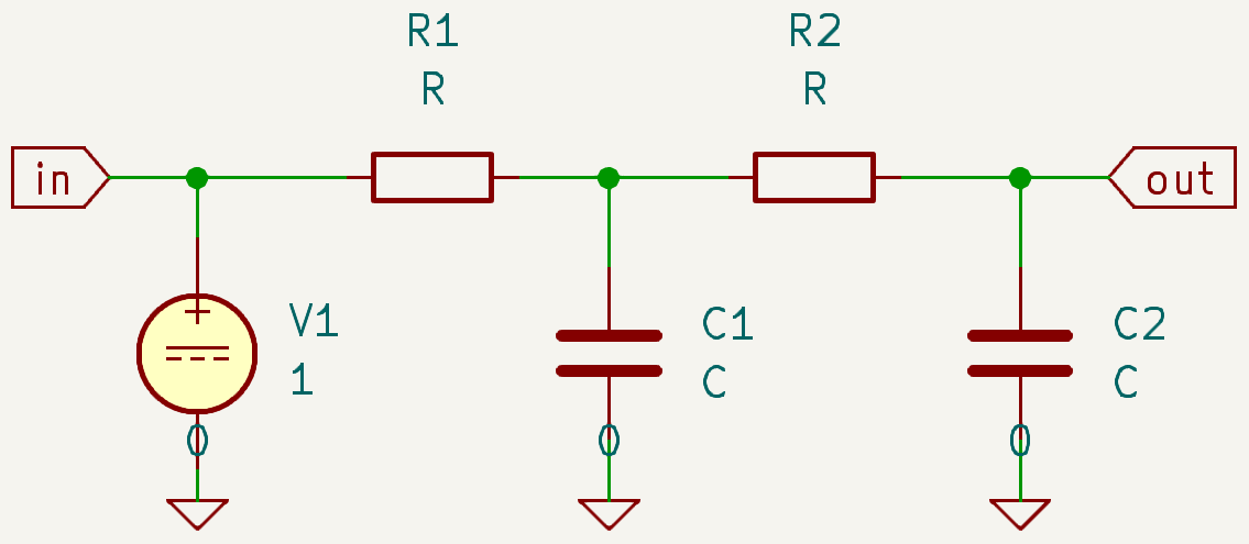
Next we have to add values to the symbols. Names with appropriate numbering (annotation) are already given to each device. Values to the resistors may be added by double click onto the 'R' and entering the value into the edit box, same with 'C'. VDC is special because it has to deliver the ngspice input. For an ac simulation we don't care for the dc value (set it to 0), but we have to enable the small signal ac input. This is achieved by double click onto the symbol, then button 'Simulation Model...'. In the 'Parameter' table, set dc value to 0 and AC magnitude (AC) to 1. then hit o.k.
Fig.2 now shows the complete input.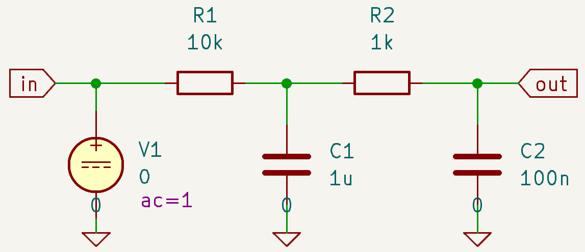
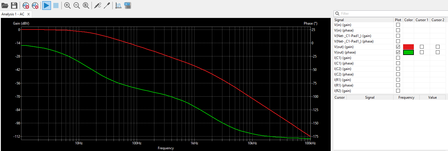
Finally we have to tell ngspice what to simulate. We want an AC simulation, which is the small signal response of the circuit to a varying frequency. We want the frequency ranging from 1 Hz to 100 kHz with 10 simulation points per decade. A simple way to tell this to the simulator is just placing a text line '.ac dec 10 1 100k' into our eeschema drawing window (see ngspice manual, chapt. 15.3.1).
There is, however, a more comfortable way (without the need to having a look at the ngspice manual). Open the simulator window with Eeschema -> Inspect -> Simulator. The simulator window pops up. Choose button "New Analysis Tab" or Ctrl+N. Select "AC - Small Singnal Ananlysis" from the "Analysis type" drop dwon menue. Enter the values for Number, Start and Stop (10 1 100k from above). On the right, select V(0ut) (gain) and V(out) (phase) for plotting. Run the simulation by hitting the (R) button. Immediately you see the simulated gain and phase of the "out" node (Fig.3), reflecting the two RC poles we have in the circuit.
As a next test we are interested in a transient simulation. All signals shall now be computed versus time.
First we have to change the input voltage signal. A step voltage from 0 to 5 V is intended. This will be available (see ngspice manual chapt. 4.1.1) with the PULSE voltage source. Open the "Choose symbol" window by the "Add symbols" button. Type VPULSE into the filter edit box, get the VSOURCE and use it to replace the VDC source in your circuit. We want the input voltage rising from 0 to 5 V after a delay of 2 us. Rise and fall times are set to 1 us as well. Pulse width and repetition time are 1s, and thus are far beyond the simulation time of 100 ms. So within our simulation time we will see only the rising edge of the input signal.
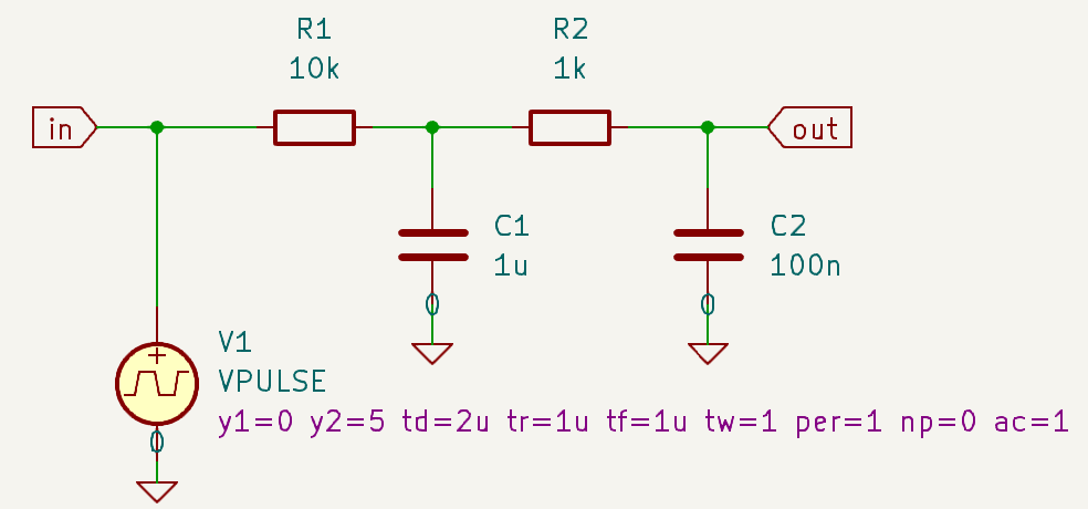
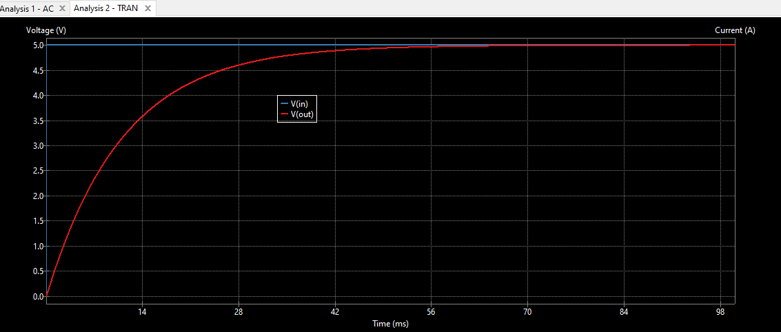
The simulation command now shall contain 100 us step size and a final time of 100 ms. So open again the "New Analysis Tab" window, now select "tran" from the drop-down menue and enter step and final time. After running the simulation (button (R)), the output (V(out) plotted versus time) does show the expected behavior, rising from 0 to 5 V, and is shown in Fig.5.
3) Bipolar amplifier
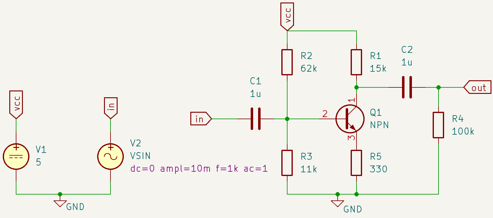
The next example is a bipolar amplifier. Two resistors R2, R3 determine the base current, R1 is the dc load, R5 provides some negative feedback. R4 is required because ngspice will not accept a capacitor that does not have a dc connection at each terminal (node "in" uses V2 for this purpose). The transistor symbol NPN stems from the Simulation_Spice library. It already involves internally provided model parameters and has a ngspice compatible pin number sequence 1, 2, and 3 for C, B, and E. The GND symbol is equivalent to the "0" symbol. The circuit is shown in Fig. 6.
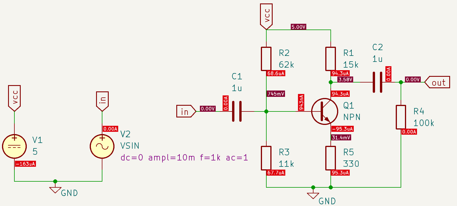
The first simulation now will be the determination of an operating point, with all voltages applied and the resulting currents simulated. Thus open the "Spice Simulator" window, open the "New Analysis Tab (ctrl N), and acknowledge to run a DC operating point. The plot window now states that there will be no plot (because you will obtain only a single operating point). After running the op simulation, have a look at the circuit window (Fig. 7):
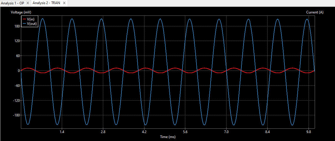
Let's now do a transient simulation (TRAN) in addition to the OP. Check the input voltage source VSIN: its amplitude is only 10 mV. Hit again the "New Analysis Tab (ctrl N), select transient (TRAN) from the dropdown menue, and add the required parameters: time step size 10u, final time 10m. The plot window will show up, you might add signals V(in) and V(out) for plotting. After running the simulation (button (R)), the plot is visible (see Fig. 8):
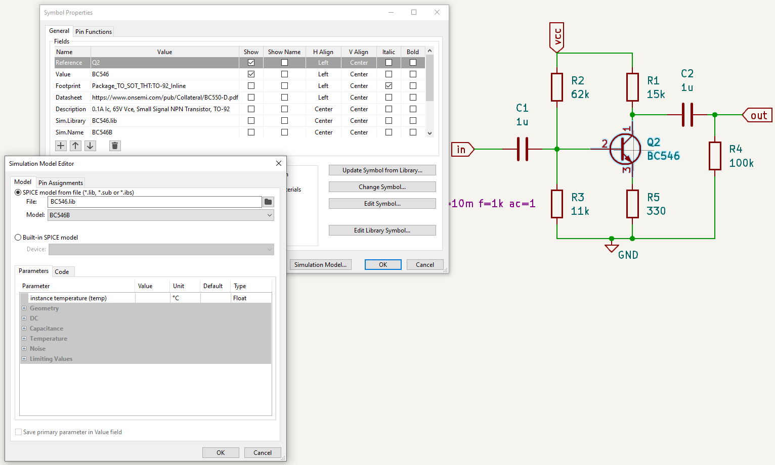
As a next step we want to replace the generic bipolar model by a suitable real world small signal NPN transistor, say the BC546. So search for the symbol (button "Add symbol" (A)) and replace the generic symbol we had in the previous example. Fortunately the new symbol has the same pin sequence (1, 2, 3 is C, B, E), so this is o.k.. The specific transistor requires a model parameter set for this device. KiCad ngspice does not provide these special device models with their distribution, you have to look for it elsewhere, e.g. at our Models for ngspice page, or others sources from the web. The basic model parameter set contains the BC546 model. Copy the BC546.lib file into your project directory. Double click onto the transistor symbol. In the "Symbol Properties" window (Fig. 9) --> Simulation Model... --> Spice Model from File --> File BC546.lib --> Model BC546B --> o.k. --> o.k..
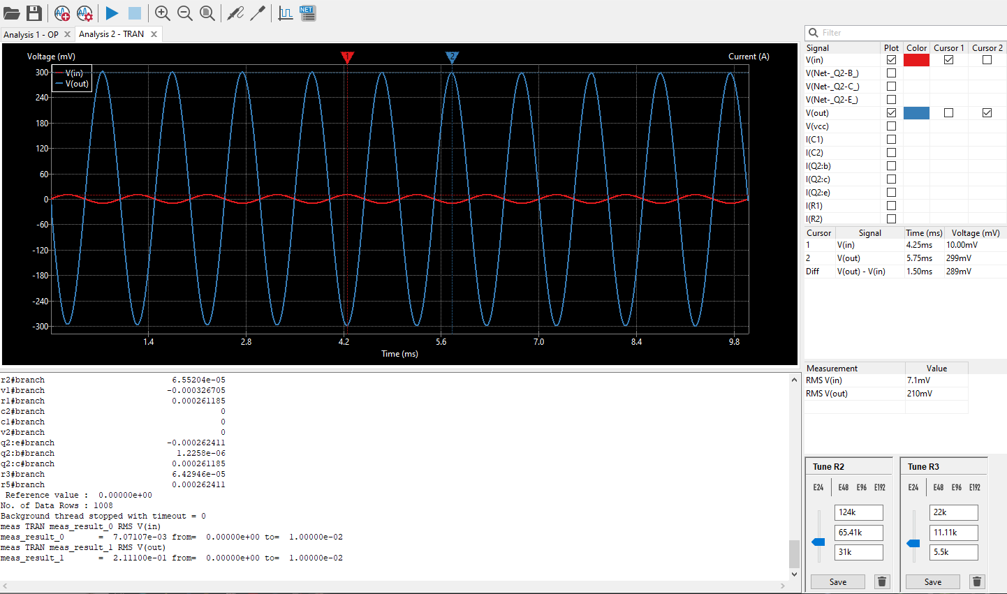
When we now run the simulation, the output voltage of the amplifier V(out) seems to be grossly distorted, not longer a true sine wave. Well, the transistor parameters are different, and thus require a different circuit bias. To achieve better amplifier performance, the values of R2 and R3 need to be optimized.
An elegant method is offered by the tuning tool. Run the transient simulation, click the "Select a value to be tuned (T)" button, select R2 and R3 on the circuit diagram and move back to the "Spice Simulator" window. Now two sliders for tuning R2 and R3 are visible (Fig. 10). As soon as we move one slider, a new simulation is started. With a little flair we may find the optimum value, and also get an idea of the sensitivity of this circuit against resistance variations.
There may be the need to use another bipolar transistor, like the BC817. Its spice model is available from industrial sources, e.g. from Diodes Inc., the symbol from the KiCad library. The circuit is shown in Fig. 9a.
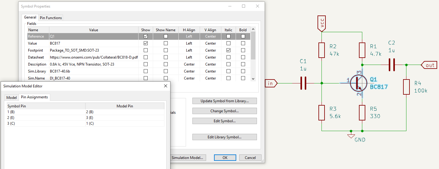
Having a closer look at the transistor symbol, we now see that the collector node is at pin 3, the base node at pin 1 and the emitter at pin 2 of the symbol. This is due to its SOT23 package. ngspice (every spice indeed) however requires a different pin numbering, namely collector at 1, base at 2, and emitter at 3. So we need some translation between KiCad symbol and ngspice, the pin assignment.
After attaching the model, as described above, open the 'Pin Assignments' window in the 'Simulation Model Editor'. On the left you will find the 'Symbol Pin' column, derived from the symbol on the Eeschema canvas and thus is fixed. On the right there is the 'Model Pin' column, which has to be modified, so that collector meets collector in the same row, base meets base and emitter meets emitter. The result is shown in Fig. 9a.
Btw. if you deal with discrete three pin MOSFETs, the sequence required by ngspice is drain (1), gate (2) and source (3). However, if you have attached a subcircuit model (often used for power MOS), then the pin sequence is determined by the model (its .subckt line), not by ngspice. For an example (with OpAmp) see chapter 5 below.
4) Inverting amplifier with generic OpAmp
The next example presents a simple inverting amplifier using an Operational Amplifier. The circuit is shown in Fig. 11. To set it up, we have used the Opamp symbol from the Simulation_SPICE library (which includes the model), generic resistors R, two VDC voltage sources for power, and a VSIN source (all three from Simulation_SPICE symbol library). The resistance ratio R2/R1 = 10 sets the amplification.
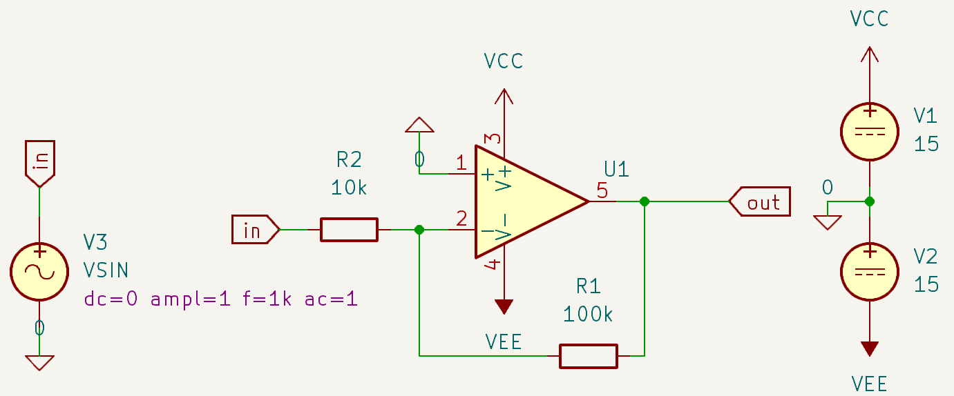
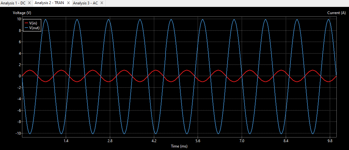
We may set up three different simulations in the Spice Simulator window, using three times the "New Analysis" (crtl N) button: a DC simulation (varying V3 from -0.1 to 0.1 with step 0.01, a TRAN (transient) simulation with time step 10u and final time 10m, and an AC simulation with 10 points per decade, start 1 and stop 1 Meg. The resultas are shown in Figs. 12 to 14.
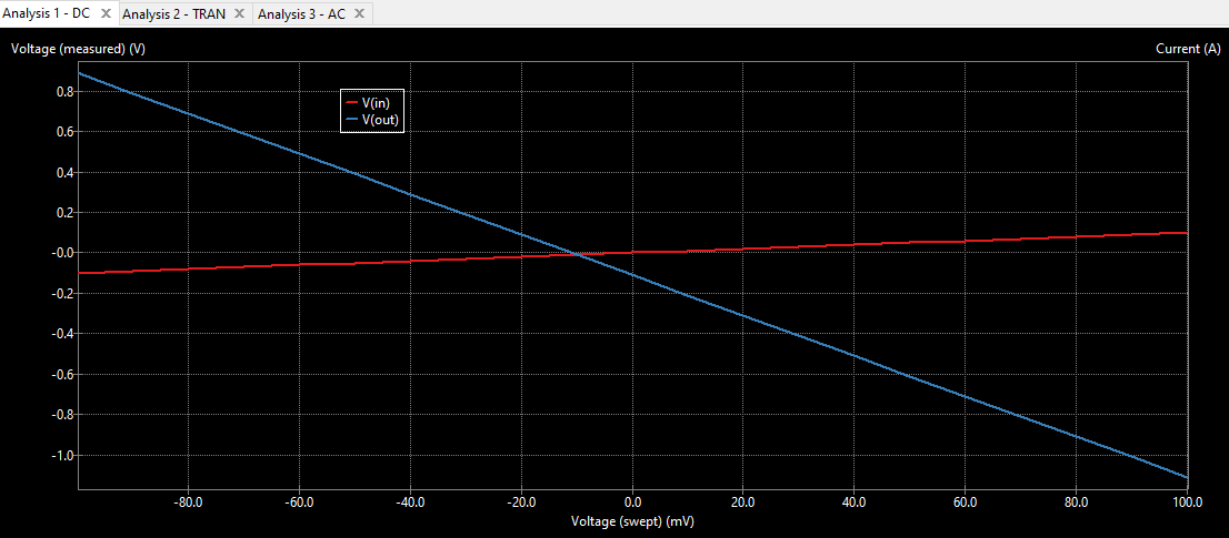
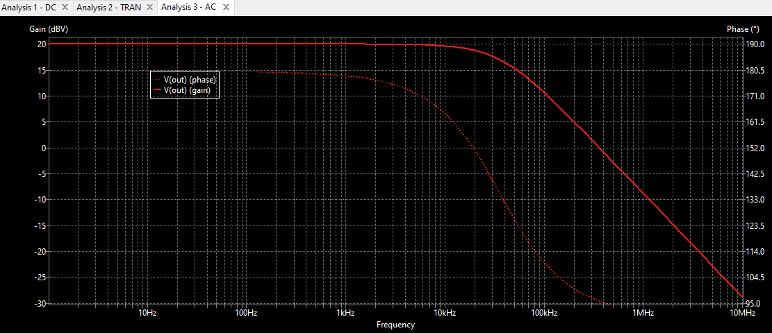
The simulation setting '.dc Vin -0.1 0.1 0.01' results in a linear Vout with a negative slope of -10. You may also notice the relatively large dc offset voltage (which is a user definable parameter of the generic opamp). The simulation setting '.ac dec 10 100 !Meg' yields the amplification degrading with increasing frequency.
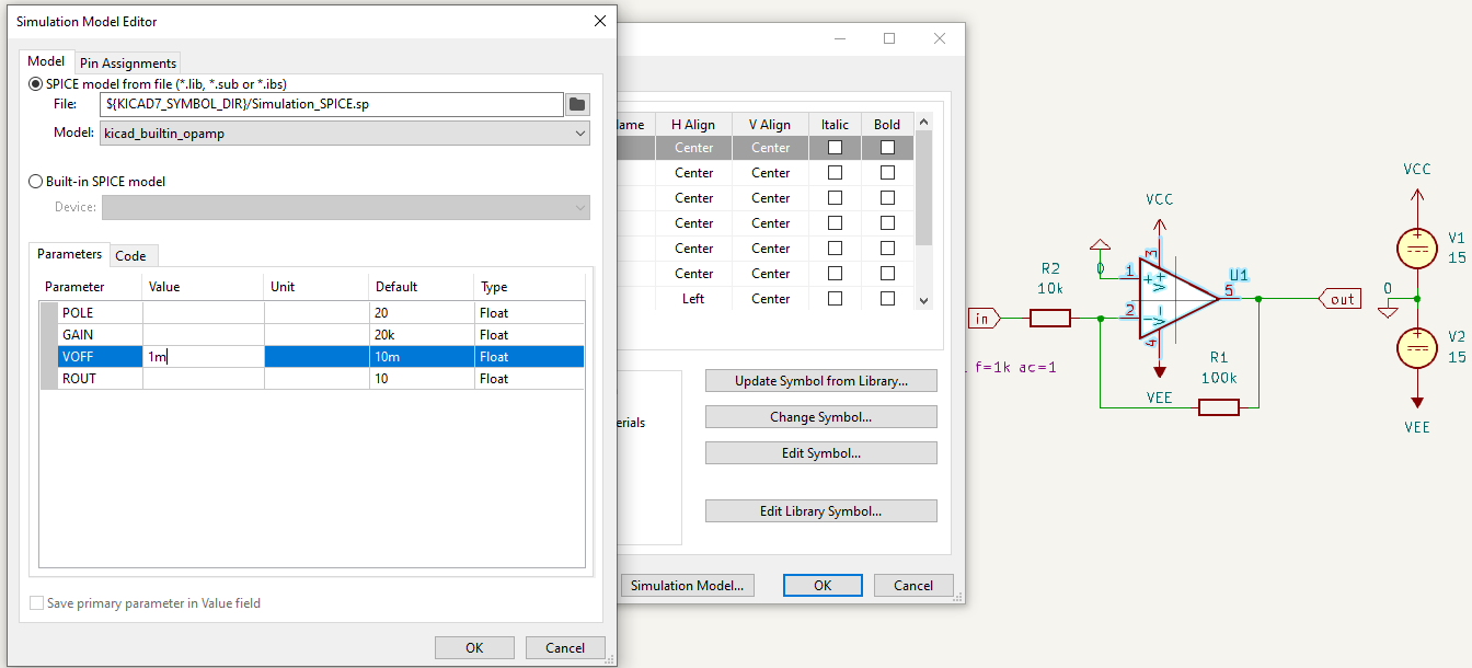
How to change parameters of the generic opamp model? The model offers 4 parameters, accessible through double-click onto the symbol, click onto "Simulation Model...", POLE (single pole frequency response), GAIN (open loop gain), VOFF (offset voltage), and ROUT (output resistance). Change a value (Fig. 15) and re-run the simulation.
5) OpAmp OPA1641
Now we want to simulate a "real world" operational amplifier, like the low noise audio amp OPA1641. Unfortunately there is no model for OpAmps delivered with ngspice. Nor does KiCad deliver such a model. So you have to search in the web for a device maker's model, e.g. from the TI web pages as PSPICE model for OPA1641, where you have to extract OPA164x.LIB and put it into directory of your choice. Common sources for models are assembled at our ngspice model page.
If you have a look at OPA164x.LIB, there you find the circuit assembled in a subcircuit (.subckt line) with name OPA164x and 5 connecting nodes.
How to add the ngspice model? Double click on the OPA1641 symbol in the circuit drawing. The 'Symbol Properties' window opens. Call 'Simulation Model...'. Select 'Model' -> 'Spice Model from File'. Enter path/name of OPA164x.LIB (for example /sim/mymodels/OPA164x.LIB). Select 'Model' -> 'OPA164x'.
Another issue has to be addressed: The pin numbering of the model description does not
comply with the pin numbering of the KiCad OPA1641 symbol U1. The KiCad symbol/pin pairs are
(in)-/2 (in)+/3 V+/7 V-/4 out/6. To start pin assignment, open the "Pin Assignment" window in the
"Simulation Model Editor". The "Reference" window does show the model text. Scroll down
until the line .SUBCKT OPA164x IN+ IN- VCC VEE OUT becomes visible.
According to the .subckt line in OPA164x.LIB the model requires a pin sequence
- non-inverting input (IN+)
- inverting input (IN-)
- positive power supply (VCC)
- negative power supply (VEE)
- output (OUT)
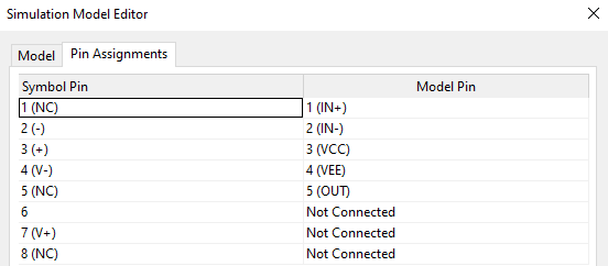
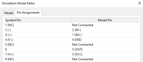
The symbol pins are given in the left column of Fig. 16a, the sequence of the model pins has to be transformed to match the symbol pins. Fig. 16a shows the starting sequence after loading the model, Fig. 16b the final solution, which is then used to create the proper ngspice netlist entry.
 |
 |
| Fig. 16a | Fig. 16b |
6) Using a Dual OpAmp TL072
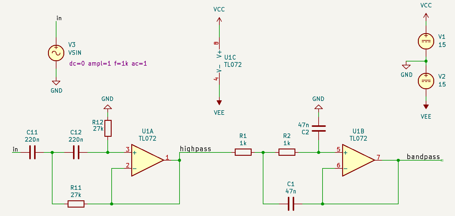
As already seen in chapt.5, KiCad symbols and Spice model files often do not fit. Especially if multi-part devices are designed in, there has to be some intermediate action. Here as an example we want to set up a bandpass filter that adds two Sallen-Key filters. Such a low pass filter is distributed with KiCad in the folder "KiCad\share\kicad\demos\simulation\sallen_key". The bandpass will need two Sallen-Keys in series, on high-pass and one low-pass filter with suitable cut-off frequencies.
For designing the filter, we need two operational amplifiers. It is reasonable to select a dual OpAmp, e.g. a TI TL072 that contains two amplifiers in an 8 pin package. Start the design in Eeschema by selecting the TL072 from the Amplifier_Operational library. Place all three units (UnitA as ampflifier 1, UnitB as amp 2, and UnitC as the power pins). Select the passives, connections, ground, input voltage and power supply, as shown in fig. 17.
You need to add the spice model for the opamp. Download the model TL072.301 from the TI web pages. Unfortunately the model has only 5 pins (in+, in-, v+, v- and out). However according to the TL072 data sheet and your circuit design you will need 8 pins (1in+,1in-, v+, v-,1out, 2in+, 2in-, and 2out) and need calling the opamp model twice, because we have two amplifiers in our circuit. So you cannot use the TI model TL072.301 directly, but need to convert it into a 2-opamp model version, as the TL072 contains two opamps. The following code sequence demonstrates how this is done by a ngspice subcircuit. Put the code into a file TL072-dual.lib, store it in the same folder as the TL072.301.
* A dual opamp ngspice model
* file name: TL072-dual.lib
.subckt TL072c 1out 1in- 1in+ vcc- 2in+ 2in- 2out vcc+
.include TL072.301
XU1A 1in+ 1in- vcc+ vcc- 1out TL072
XU1B 2in+ 2in- vcc+ vcc- 2out TL072
.ends
The .subckt line contains 8 subcircuit nodes, following after the ".subckt" token and the subcircuit name. The sequence of these nodes (1out 1in- 1in+ vcc- 2in+ 2in- 2out vcc+) is chosen so that it fits the TL072 pin number sequence (1 2 3 4 5 6 7 8) as given in the data sheet. The .include line includes the TI model. The XU1A and XU1B lines are the instantiations of the two amplifiers. Their node sequence is determined by the model (see file TL072.301). Amp 1 uses 1out 1in- 1in+, amp 2 uses 2in+ 2in- 2out, the power pins are common for both amps. In fact the subcircuit transfers the pin numbers 1 - 8 via the nodes on the .subckt line to the proper nodes in the model.
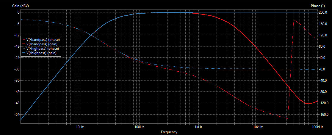
You will need to add TL072-dual.lib as a subcircuit model to one unit of the amplifier IC (now called U1A, U1B and U1C in the Eeschma circuit drawing). This is done by double clicking onto the unit, and then selecting the button "Simulation Model..." --> Model --> "Spice Model from File", adding TL072-dual.lib and choosing model TL072c. Eeschema automatically generates an instance of the complete TL072 with its nodes 1 - 8. Thus no alternative pin assignmant is required during editing the spice model in eeschema. If done, you are ready for simulating. The ac simulation result of the /bandpass node (magnitude in dB and phase in degrees versus frequency) is presented in Fig. 17.
B.t.w.: The original model file TL072.301 from TI contains a non-printable character in its last line. While ngspice for Windows does not care, ngspice for Linux will stumble over it. Just remove this character. A fix to do this automatically has been committed.
7) Digital Simulation
ngspice offers true mixed-signal simulation capability, that is analog simulation, as we have seen above, plus digital simulation. Digital simulation is fast, as it involves handling of lists with events and their time. No matrix shuffling and solving is required. The disadvantage of this approach is that we get logic signals versus time, including their delays, but no detailed analog voltage and current waveforms. The interface between analog and digital is automatic, no extra handling is needed.
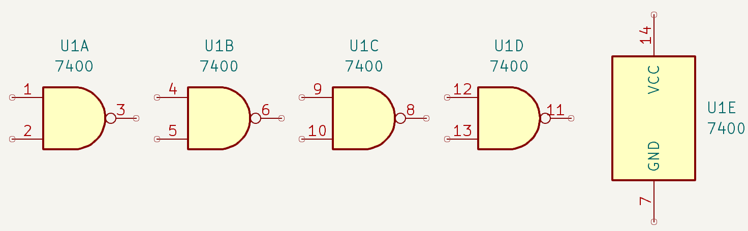
For digital modeling of standard devices like the 74xx or 40xx series ngspice uses the so-called U devices, which have been introduced by PSPICE or MicroCap. Model parameters are available at the Models for ngspice page, especially in this subset. Models ready for easy use, including pin assignment, and multipart translation are available at 74HCxxxM.7z.
7.1) Prepare the digital models
There is a caveat, though. Whereas for example the ngspice model for the 7400 NAND gate has only 3 pins (2 in, 1 out), the KiCad symbol for the 7400 has 14 pins (4 times a NAND gate, plus power and ground). There is an action required as already shown in the previous chapter. We need a subcircuit for the pin assignment, for translating the model's pins to the symbol's pins. But we need to do this only once for each new device we want to use in our simulation, it afterwards may be re-used for all simulations following. We have done this already for a few devices (NAND, NOR, INV, DFF, ...) to be found at 74HCxxxM.7z. However, for the many devices still lacking multi-gate pin assignment, the following is a hint how to proceed.
Let's start with a subcircuit.
.subckt 74HC00m 1 2 3 4 5 6 7 8 9 10 11 12 13 14
.ends
This is our frame, .subckt is the beginning of the model description, .ends is its end. The subcircuit
name is 74HC00m. And then we have the14 pins.
Next we add the NAND model from 74xx-models.7z, choosing the HC variant (which still seems to be
available from distributors).
.subckt 74HC00m 1 2 3 4 5 6 7 8 9 10 11 12 13 14
*
.SUBCKT 74HC00  1A 1B 1Y
+     optional: DPWR=$G_DPWR DGND=$G_DGND
+     params: MNTYMXDLY=0 IO_LEVEL=0
U1 nand(2) DPWR DGND
+     1A 1B 1Y
+     DLY_HC00 IO_HC MNTYMXDLY={MNTYMXDLY} IO_LEVEL={IO_LEVEL}
.model DLY_HC00 ugate (tplhTY=9ns tplhMX=18ns tphlTY=9ns tphlMX=18ns)
.ENDS  74HC00
*
.ends
How get to know what the pins 1 to 14 are used for? Well, have a look at the data sheet, or better grab the symbol and place it with all component onto the Eeschema canvas and have a look:
Now we have to call 74HC00 four times inside of 74HC00m and check that each 1A 1B 1Y of 74HC00 maps correctly onto 1 - 14 of 74HC00m.
.subckt 74HC00m 1 2 3 4 5 6 7 8 9 10 11 12 13 14
*
* ----------------------------------------------------------- 74HC00 ------
*  Quad 2-Input Nand Gates
*
.SUBCKT 74HC00  1A 1B 1Y
+     optional: DPWR=$G_DPWR DGND=$G_DGND
+     params: MNTYMXDLY=0 IO_LEVEL=0
U1 nand(2) DPWR DGND
+     1A 1B 1Y
+     DLY_HC00 IO_HC MNTYMXDLY={MNTYMXDLY} IO_LEVEL={IO_LEVEL}
.model DLY_HC00 ugate (tplhTY=9ns tplhMX=18ns tphlTY=9ns tphlMX=18ns)
.ENDS  74HC00
*
Xnand1 1 2 3 74HC00
Xnand2 4 5 6 74HC00
Xnand3 9 10 8 74HC00
Xnand4 12 13 11 74HC00
.ends
For this event based digital simulation we don't need the power pins 7 and 14, so just ignore them.
Finally put this subcircuit into a file 74HC00.lib for using it in the following examples.
The procedure described above has been used to generate a small (but growing) number of 74HCxxx gates. We have INV, NAND, NOR, XOR, and DFF, to be downloaded from our ngspice model page as 74HCxxxM.7z.
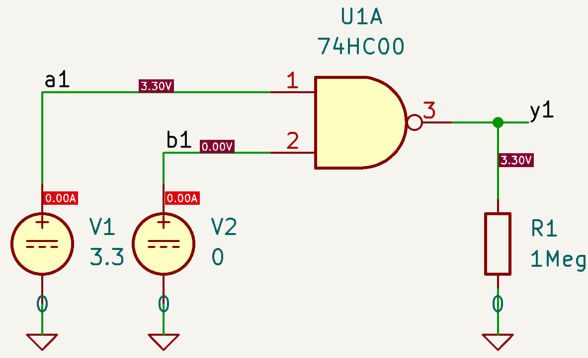
7.2) Simple NAND gate example
Let us start with simulating a simple NAND gate. Grab the symbol, but place only its first part U1A and discard the rest. Attach our model from file 74HC00.lib (Eeschema --> Double click onto U1A --> Simulation Model... --> Model SPICE from file --> select File: 74HC00.lib --> Model: 74HC00m --> ok --> ok.). For the input we use two VDC from library Simulation_SPICE. These are analog DC voltage sources, ngspice cares automatically for the interface to the digital event world. ngspice assumes a supply voltage of 3.3 V for the digital devices, so the analog input shall have the same value (3.3 V if you want to enter a "1" signal, 0 V if to enter "0"). If you want a different supply (within the limits of the data sheet), e.g. 5 V, put this statement ".param vcc=5" into a text box onto the Eeschema canvas. Analog input voltages have to be tailored accordingly. The resistor R1 is required to translate the output back from digital to analog. Unfortunately currently Eeschema cannot list or plot the digital data directly.
For simulation we use a quick operating point (OP) sim (Eeschema --> Inspect --> Simulator --> New Ananlysis (ctrl N) --> OP --> unselect "Save all currents" and "Save all power dissipations" --> ok. --> Run simulation (R). On the canvas (Fig. 20) you see the resulting input and output voltages. If you change the input, the output will follow after a new simulation.
7.3) Full adder made with NAND gates
The next circuit is a little bit more complex, a 2-bit full adder made from NAND gates we have already used in the previous chapter. It has three inputs, the two values to be added and the carry-in bit (from a potential previous adder stage). Two outputs are the sum and carry-out.
Generally, for a digital simulation, we need three items: A stimulus which provides adequate signals to stimulate the second item, the device under test, and thirdly we need some means to read and review the resulting data. Even for such a small circuit as shown in Fig. 21 with only three inputs and 2 outputs we need 8 input combinations (or "words") to achieve a full logic test. In the example in Fig. 21 we use 3 pulsed voltage sources and a transient (voltage versus time) simulation. This is not meant to extract timing data, but just to cover all 8 input combinations.
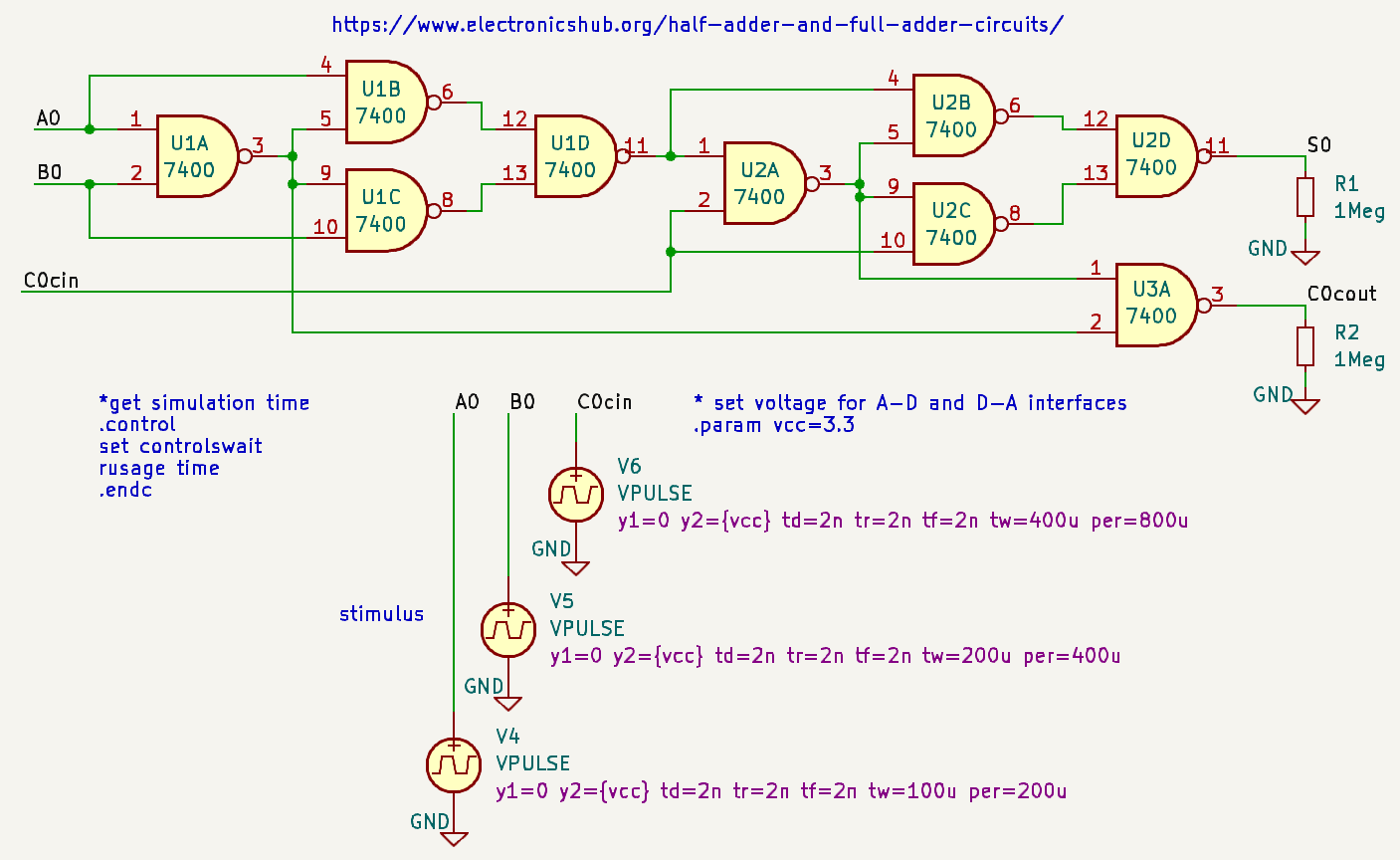
The input/output plot in Fig. 22 plots the three inputs and the two outputs on top of each other, like this was a digital plot. The lower three signals are the pulsed voltage sources, and their timing is chosen so that all input combinations are covered. You may check if the output reflects the truth table given in the literature (it does).
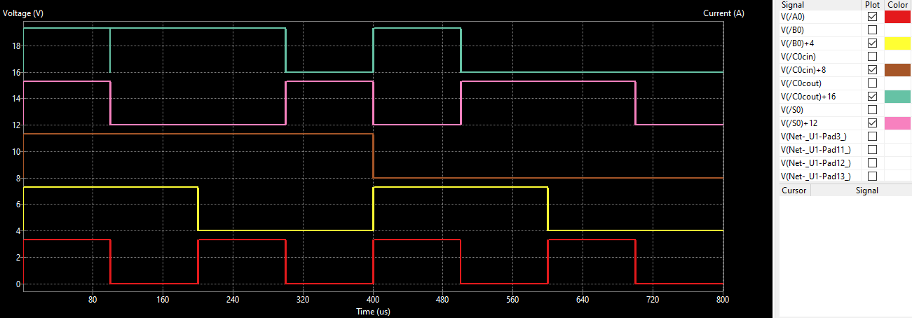
Fig. 21 reveals some "tricks" used. The parameter "vcc" has been set, not only for the digital circuitry, but also for the stimuli, as {vcc} is replaced by the .param value. R1 and R2 are used to translate the digital data to the analog world. The simulation time is measured with the text box insert (*get the sim...). On my machine it is a mere 4 ms. The plot in Fig. 22 has been achieved by not plotting the signals directly (they would obscure each other in a single row), but plotting user-defined signals ("Spice Simulator" window --> Simulation --> User-defined signals), adding n*4 (n is 0 to 4) to each signal.
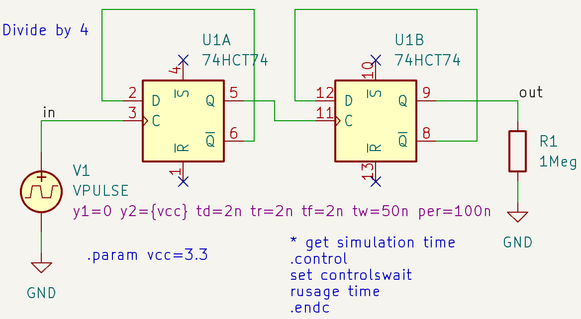
7.4) Divide by 4 with D-FF
The "Divide by 4" circuit uses 2 D flip-flops, which are available as 7474 in a single 14 pin package. So we again have to design a subcircuit to match the model 74HC74 with 6 pins to the symbol with 14 pins. It is the same procedure as has been described above. In the .subckt line of the final model 74HC74M we have not used just numbers, but the pin names, in their correct sequence, thus corresponding to the pin numbers 1 to 14.
The procedure towards the simulation is now the same as described above: Draw the circuit (set, reset and power pins are not used), attached the subciruit model 74HC74M to the symbol, define appropriate user-defined signal for plotting, set the transient plot data (time step 2n, final time 2u, not using "Save all currents" nor "Save all power dissipations") and run the simulation.
.subckt 74HC4M _R1 D1 C1 _S1 Q1 _Q1 VGND _Q2 Q2 _S2 C2 D2 _R2 VCC

* ----------------------------------------------------------- 74HC74 ------
*  Dual D-Type Positive Edge Triggered Flip-Flops With  Preset And Clear
*
*
.SUBCKT 74HC74 1PREBAR 1CLRBAR 1CLK 1D 1Q 1QBAR
+     optional:  DPWR=$G_DPWR DGND=$G_DGND
+     params:  MNTYMXDLY=0 IO_LEVEL=0
U1 DFF(1) DPWR DGND
+     1PREBAR 1CLRBAR 1CLK 1D 1Q 1QBAR
+     DLY_HC74 IO_HC MNTYMXDLY={MNTYMXDLY} IO_LEVEL={IO_LEVEL}
.model DLY_HC74 ueff(tppcqlhTY=20ns tppcqlhMX=46ns tppcqhlTY=20ns
+                 tppcqhlMX=46ns twpclMN=25ns
+                 tpclkqlhTY=20ns tpclkqlhMX=35ns tpclkqhlTY=20ns
+                 tpclkqhlMX=35ns twclkhMN=20ns twclklMN=20ns
+                 tsudclkMN=25ns tsupcclkhMN=6ns)
.ENDS 74HC74

XUA  _S1 _R1 C1 D1 Q1 _Q1 74HC74
XUB  _S2 _R2 C2 D2 Q2 _Q2 74HC74
.ends
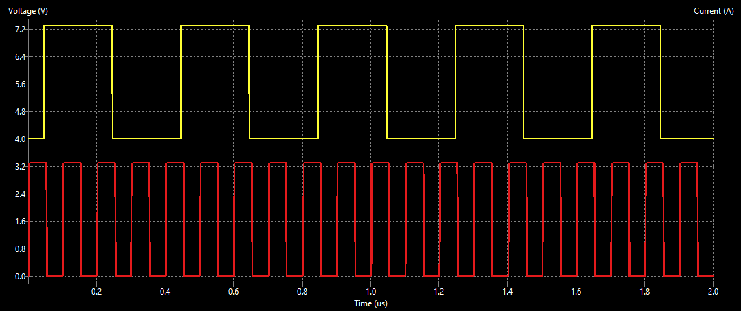
The simulation result (input and output signal) in Fig. 24 indeed does show the "divide by 4" action of this circuit.
8) Using external ngspice
For MS Windows needs to be fixed in Eeschema
9) Enhancing the script for use with both internal or external ngspice
For MS Windows needs to be fixed in Eeschema
10) Links to models, videos etc.
Here you will find some links: our model parameters page contains a large amount of models and model parameters. The two collections are early complete and will serve many of your needs, and if you have a special request, there are links to semiconductor vendors' model pages as well.
The project files for chapters 2 to 6 are found here.
Links to Eeschema/ngspice examples:
39 example projects (KiCad 6.0.2, ngspice-36) are assembled here.
24 example projects (KiCad 8 RC2, ngspice-42) are presented here (more to come).
Links to Eeschema/ngspice manuals:
- Official Eeschema/ngspice manual for version 8.0.7.
- ngspice manual.
- KiCad Tips And Tricks / Simulation.
Below there are some introductory videos for KiCad/ngspice (update to KiCad8 is needed):
